Difference between revisions of "System deployment"
| Line 1: | Line 1: | ||
TODO: descrizione uart_router, memory_controller, con riferimento a template nexys4ddr, (comandi, console) e memoria, disegno/schema, interazione con host, loading memoria, avvio kernel | TODO: descrizione uart_router, memory_controller, con riferimento a template nexys4ddr, (comandi, console) e memoria, disegno/schema, interazione con host, loading memoria, avvio kernel | ||
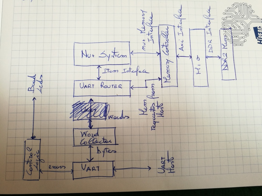
| − | The [[SC_System|Single core version]] has been deployed on a '''Nexys4DDR FPGA''' board, modules involved are located into ''boards/nexys4ddr'' and ''src/deploy/'' folders. The design interconnects the board DDR memory and the UART respectively to the Memory and Item interfaces. The figure below shows a schematic block of the top module: | + | The [[SC_System|Single core version]] has been deployed on a '''Nexys4DDR FPGA''' board, modules involved are located into ''boards/nexys4ddr'' and ''src/deploy/'' folders. The design interconnects the board '''DDR''' memory and the '''UART''' respectively to the Memory and Item interfaces. The figure below shows a schematic block of the top module: |
[[File:Nexys4DDR.jpg|900px]] | [[File:Nexys4DDR.jpg|900px]] | ||
Revision as of 19:00, 14 May 2019
TODO: descrizione uart_router, memory_controller, con riferimento a template nexys4ddr, (comandi, console) e memoria, disegno/schema, interazione con host, loading memoria, avvio kernel
The Single core version has been deployed on a Nexys4DDR FPGA board, modules involved are located into boards/nexys4ddr and src/deploy/ folders. The design interconnects the board DDR memory and the UART respectively to the Memory and Item interfaces. The figure below shows a schematic block of the top module:
The nuplus_system lays on the middle of the design, while uart_router and memory_controller translate nu+ transactions letting the system communicate with both the host (through the UART) and with the board memory (through the DDR interface).
Memory Controller
da AXI a DDR The memory controller deployed in the current release translates incoming memory requests on the Memory Interface into AXI transactions, forwarded to the MIG IPCore instantiated into the design. The memory_controller provides to the nuplus_system a block interface compliant with the core Memory Interface:
// Block interface
input  logic [31 : 0]               blk_request_address,
input  logic [63 : 0]               blk_request_dirty_mask,
input  logic [511 : 0]              blk_request_data,
input  logic                        blk_request_read,
input  logic                        blk_request_write,
output logic                        mc_available,
output logic                        mc_response_valid,
output logic [31 : 0]               mc_response_address,
output logic [511 : 0]              mc_response_data,
input  logic                        blk_available,
Turning nu+ memory requests into AXI transactions:
// AXI write address channel signals
input                               axi_awready, // Indicates slave is ready to accept
output logic [3:0]                  axi_awid,    // Write ID
output logic [31:0]                 axi_awaddr,  // Write address
output logic [7:0]                  axi_awlen,   // Write Burst Length
...
Then, the MIG turns incoming AXI requests into DDR transactions forwarded to memory blocks located on the board.
The memory_controller also generates the memory availability bit. It instantiates a FIFO input_fifo in which incoming requests from the nuplus_system are stored. The input_fifo stores incoming request data and information, such as address, when either blk_request_read or blk_request_write are valid:
sync_fifo #(
 .WIDTH                 ( 32 + 64 + 512 + 1 + 1 ),
 .SIZE                  ( 2 ),
 .ALMOST_FULL_THRESHOLD ( 1 )
) input_fifo (
 .clk          ( clk ),
 .reset        ( reset ),
 .flush_en     ( 1'b0 ),
 .full         ( ),
 .almost_full  ( input_fifo_almost_full ),
 .enqueue_en   ( blk_request_read | blk_request_write ),
 .value_i      ( {blk_request_address, blk_request_dirty_mask, blk_request_data, blk_request_read, blk_request_write} ),
 .empty        ( input_fifo_empty ),
 .almost_empty ( ),
 .dequeue_en   ( fifo_blk_dequeue ),
 .value_o      ( {fifo_blk_request_address, fifo_blk_request_dirty_mask, fifo_blk_request_data, fifo_blk_request_read, fifo_blk_request_write} )
);
The availability signals is deasserted when input_fifo has an element stored:
assign mc_available = ~input_fifo_almost_full;
When the AXI transaction is closed and all input words are gathered back into a single block (512-bit):
READ_BLOCK: begin
  if (axi_rvalid) begin
    word_counter <= word_counter + 1;
    mc_response_data[word_counter * 32 +: 32] <= axi_rdata;
  ...
Finally, the control logic dequeues the pending request asserting fifo_blk_dequeue and forward the memory response to the nuplus_system.
The memory_controller also bridges the uart_router (receiving commands from the host) and the board memory. It provides a Command interface directly interconnected with uart_router, this interface allows the host to interfact with the memory through commands flowing on the UART:
// Command interface
input  [31:0]                       command_word_i,
input                               command_valid_i,
output logic                        command_ready_o,
output logic [31:0]                 command_word_o,
output logic                        command_valid_o,
input                               command_ready_i,
The Command interface has a valid/read interface such as the nuplus_system. When the host issues a memory request through the UART, uart_router asserts command_valid_i and forwards address and operation type on command_word_i. In particular, the FSM checks the most significant bit of command_valid_i, if low a READ request is issued, otherwise the FSM performs a WRITE memory request:
case (current_state)
 IDLE: begin
  if (command_valid_i) begin
   is_read       <= command_word_i[31] == READ;
In case of READ, an AXI transaction is performed and no data is needed. In case of WRITE, the FSM gathers the next 15 incoming command_word_i and keep sending them through the AXI write channel:
WRITE_BURST: begin
  axi_wdata                         <= command_word_i;
  axi_wstrb                         <= 4'b1111;
 if (command_valid_i & axi_wready) begin
   axi_wvalid                      <= 1'b1;
   command_ready_o                 <= 1'b1;
   if (word_counter == burst_len - 1) begin
     axi_wlast                     <= 1'b1;
   end
 end
end
The burst ends when 16 words have been sent over the AXI write channel and axi_wlast is asserted.
Host interaction
Uart controller e traduzione in items per nu+ (da uart_router)
Console commands
uart_loader.py
